
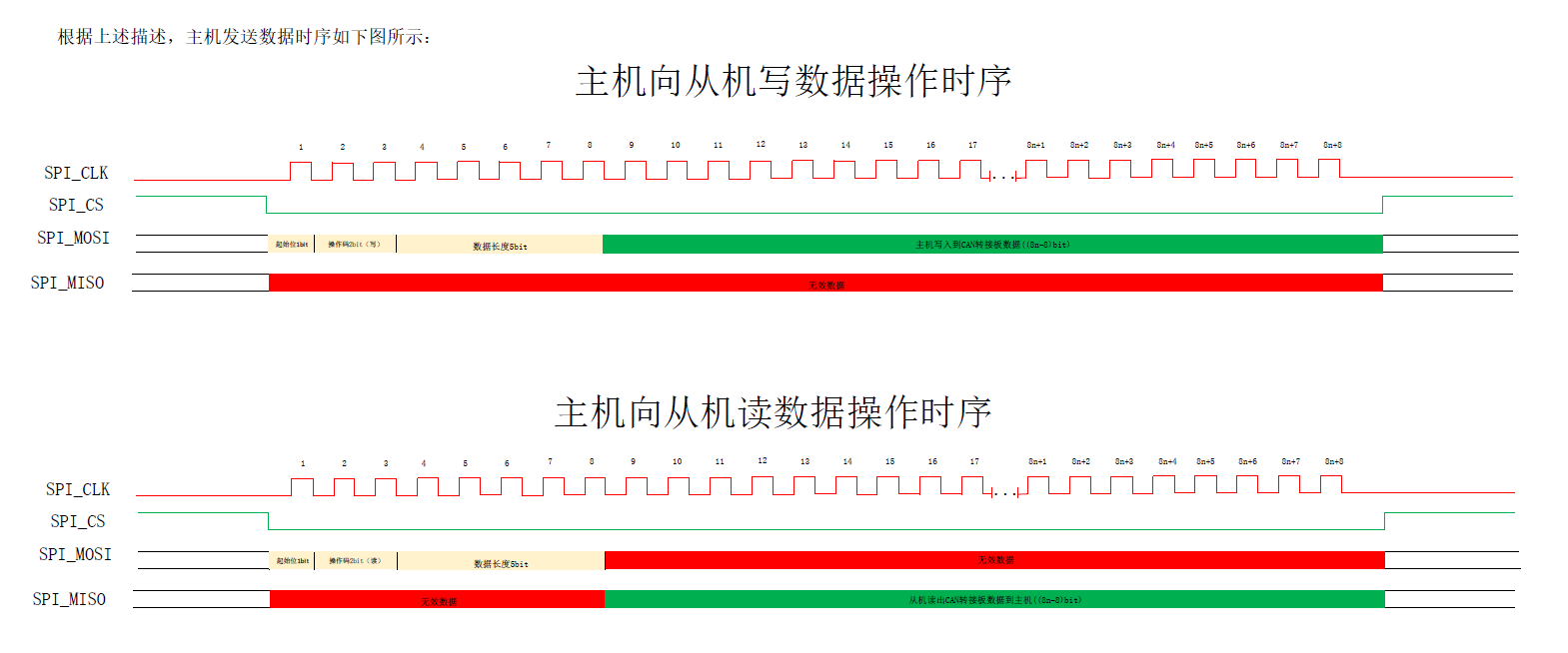
大家好,又见面了,我是你们的朋友全栈君。如果您正在找激活码,请点击查看最新教程,关注关注公众号 “全栈程序员社区” 获取激活教程,可能之前旧版本教程已经失效.最新Idea2022.1教程亲测有效,一键激活。
Jetbrains全系列IDE稳定放心使用
SPI 协议是由摩托罗拉公司提出的通讯协议(Serial Peripheral Interface),即串行外围设备接口,是一种高速全双工的通信总线。它被广泛地使用在 ADC、LCD 等设备与 MCU 间,要求通讯速率较高的场合。
SPI 通讯设备之间的常用连接方式见图 1。
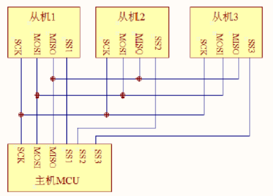

SPI 通讯使用3 条总线及片选线,3 条总线分别为SCK、MOSI、MISO,片选线为 SS
,它们的作用介绍如下:
(1) SS ( Slave Select):从设备选择信号线,常称为片选信号线,也称为NSS、CS,以下用NSS 表示。当有多个SPI 从设备与SPI 主机相连时,设备的其它信号线SCK、MOSI及MISO 同时并联到相同的SPI 总线上,即无论有多少个从设备,都共同只使用这3 条总线;而每个从设备都有独立的这一条NSS 信号线,本信号线独占主机的一个引脚,即有多少个从设备,就有多少条片选信号线。I2C 协议中通过设备地址来寻址、选中总线上的某个设备并与其进行通讯;而SPI 协议中没有设备地址,它使用NSS 信号线
来寻址,当主机要选择从设备时,把该从设备的NSS 信号线设置为低电平,该从设备即被选中,即片选有效,接着主机开始与被选中的从设备进行SPI 通讯。所以SPI 通讯以NSS 线置低电平为开始信号,以NSS 线被拉高作为结束信号。
(2) SCK (Serial Clock):时钟信号线,用于通讯数据同步。它由通讯主机产生,决定了通讯的速率,不同的设备支持的最高时钟频率不一样,如STM32 的SPI 时钟频率最大为fpclk/2,两个设备之间通讯时,通讯速率受限于低速设备。
(3) MOSI (Master Output, Slave Input):主设备输出/从设备输入引脚。主机的数据从这条信号线输出,从机由这条信号线读入主机发送的数据,即这条线上数据的方向为主机到从机。
(4) MISO(Master Input,,Slave Output):主设备输入/从设备输出引脚。主机从这条信号线读入数据,从机的数据由这条信号线输出到主机,即在这条线上数据的方向为从机到主机。
协议层
与I2C 的类似,SPI 协议定义了通讯的起始和停止信号、数据有效性、时钟同步等环节。
SPI 基本通讯过程先看看SPI 通讯的通讯时序,见图 2。
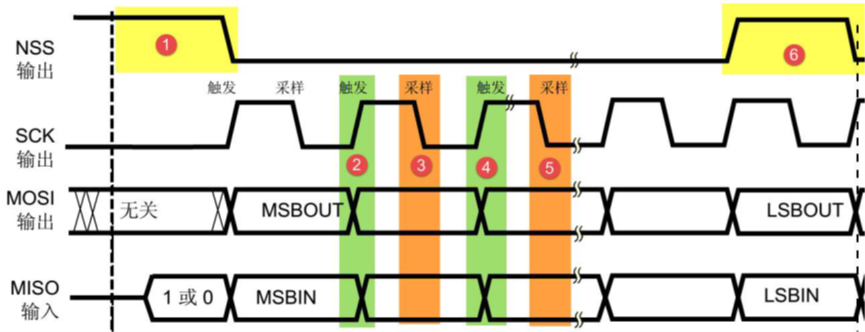
这是一个主机的通讯时序。NSS、SCK、MOSI 信号都由主机控制产生,而MISO 的信号由从机产生,主机通过该信号线读取从机的数据。MOSI 与MISO 的信号只在NSS 为低电平的时候才有效,在SCK 的每个时钟周期MOSI 和MISO 传输一位数据。以上通讯流程中包含的各个信号分解如下:
3. 通讯的起始和停止信号
在图 2 中的标号处,NSS 信号线由高变低,是SPI 通讯的起始信号。NSS 是每个从机各自独占的信号线,当从机在自己的NSS 线检测到起始信号后,就知道自己被主机选中了,开始准备与主机通讯。在图中的标号处,NSS 信号由低变高,是SPI 通讯的停止信号,表示本次通讯结束,从机的选中状态被取消。
4. 数据有效性
SPI 使用MOSI 及MISO 信号线来传输数据,使用SCK信号线进行数据同步。MOSI 及MISO 数据线在SCK 的每个时钟周期传输一位数据,且数据输入输出是同时进行的。数据传输时,MSB 先行或LSB 先行并没有作硬性规定,但要保证两个SPI 通讯设备之间使用同样的协定,一般都会采用图 2 中的MSB 先行模式。MOSI 及MISO 的数据在SCK的上升沿期间变化输出,在SCK 的下降沿时被采样。即在SCK 的下降沿时刻,MOSI 及MISO 的数据有效,高电平时表示数据“1”,为低电平时表示数据“0”。在其它时刻,数据无效,MOSI 及MISO 为下一次表示数据做准备。SPI 每次数据传输可以8 位或16 位为单位,每次传输的单位数不受限制。
5. CPOL/CPHA 及通讯模式
上面讲述的图 25-2 中的时序只是SPI 中的其中一种通讯模式,SPI 一共有四种通讯模式,它们的主要区别是总线空闲时SCK 的时钟状态以及数据采样时刻。为方便说明,在此引入“时钟极性CPOL”和“时钟相位CPHA”的概念。时钟极性CPOL 是指SPI 通讯设备处于空闲状态时,SCK 信号线的电平信号(即SPI 通
讯开始前、 NSS 线为高电平时SCK 的状态)。CPOL=0 时, SCK 在空闲状态时为低电平,CPOL=1 时,则相反。时钟相位CPHA 是指数据的采样的时刻,当CPHA=0 时,MOSI 或MISO 数据线上的信号将会在SCK 时钟线的“奇数边沿”被采样。当CPHA=1 时,数据线在SCK 的“偶数边沿”采样。见图 3 及图 4。
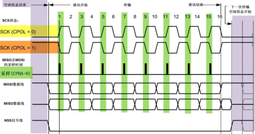
我们来分析这个CPHA=0 的时序图。首先,根据SCK在空闲状态时的电平,分为两种情况。SCK 信号线在空闲状态为低电平时,CPOL=0;空闲状态为高电平时,CPOL=1。无论CPOL=0 还是=1,因为我们配置的时钟相位CPHA=0,在图中可以看到,采样时刻都是在SCK 的奇数边沿。注意当CPOL=0 的时候,时钟的奇数边沿是上升沿,而CPOL=1 的时候,时钟的奇数边沿是下降沿。所以SPI 的采样时刻不是由上升/下降沿决定的。MOSI 和MISO 数据线的有效信号在SCK 的奇数边沿保持不变,数据信号将在SCK 奇数边沿时被采样,在非采样时刻,MOSI 和MISO 的有效信号才发生切换。类似地,当CPHA=1 时,不受CPOL 的影响,数据信号在SCK的偶数边沿被采样,见图 4。
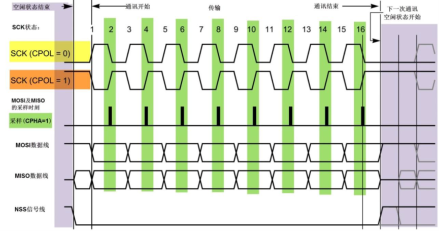
图 4 CPHA=1 时的SPI 通讯模式
由CPOL 及CPHA 的不同状态,SPI 分成了四种模式,见表 1,主机与从机需要工
作在相同的模式下才可以正常通讯,实际中采用较多的是“模式0”与“模式3”。
表 1 SPI 的四种模式
SPI 模式 CPOL CPHA 空闲时SCK 时钟 采样时刻
0 0 0 低电平 奇数边沿
1 0 1 低电平 偶数边沿
2 1 0 高电平 奇数边沿
3 1 1 高电平 偶数边沿
3 FPGA实现从机收发SPI数据
在实现SPI时需要完成通信协议和数据长度的约定,这个代码实现的协议如下图所示
代码如下所示,代码通过多时钟上升沿的变化来读写数据的
`timescale 1ns / 1ps
//
// Company:
// Engineer:
//
//
module SPI_data(
input   	wire		                clk_100m    		,
input		wire						clk_125m			,
input   	wire		                rst_n       		,

input		wire						spi_sclk0			,				//mast
input		wire						spi_cs0				,
input		wire						spi_din0			,
output		reg							spi_dout0			,


output		reg							spi_wr_flag			,
output		reg							spi_rd_flag			,
output		reg		[1:0]				spi_rd_data_id		,

input		wire						data_in_en			,
input		wire	[15:0]				data_in				,
output		reg							data_out_en			,
output		reg		[15:0]				data_out


    );

//
//SPI1

parameter			spi_data_dlc	=	14				;
parameter			spi_data_dlc_t	=	13				;
parameter			spi_dlc			=	16				;
parameter			spi_half_dlc	=	8				;

reg										spi_sclk0_t			;
reg										spi_cs0_t			;
reg										spi_din0_t			;
reg										spi_sclk0_t_t		;
reg										spi_cs0_t_t			;
reg										spi_din0_t_t		;
reg										spi_cs0_t_t_t		;

reg										data_din_flag		;
reg										one_data_flag		;
reg										one_data_flag_t		;


reg										data_dout_flag		;


reg				[6:0]					spi_bit_cont		;


reg				[4:0]					spi_cs0_cont		;
reg				[7:0]					spi_first_data0		;
reg				[7:0]					spi_last_data0		;

reg				[15:0]					spi_sum_in			;
reg				[15:0]					spi_sum_out			;

always @(posedge clk_100m or negedge rst_n )begin
if(rst_n==1'b0) begin
spi_sclk0_t		<= 'b0							;
spi_cs0_t		<= 'b0							;
spi_din0_t		<= 'b0							;
spi_sclk0_t_t	<= 'b0							;
spi_cs0_t_t		<= 'b0							;
spi_din0_t_t	<= 'b0							;
spi_cs0_t_t_t	<= 'b0							;
end else  begin
spi_sclk0_t		<= spi_sclk0					;
spi_cs0_t		<= spi_cs0						;
spi_din0_t		<= spi_din0						;
spi_sclk0_t_t	<= spi_sclk0_t					;
spi_cs0_t_t		<= spi_cs0_t					;
spi_cs0_t_t_t	<= spi_cs0_t_t					;
spi_din0_t_t	<= spi_din0_t					;
end
end

SPI modle 0 16 bit

always @(posedge clk_100m or negedge rst_n )begin
if(rst_n==1'b0) begin
spi_cs0_cont	<= 'b0							;
end else if ((spi_cs0_t_t==1'b0)&&((spi_sclk0_t_t==1'b0)&&(spi_sclk0_t==1'b1))) begin
spi_cs0_cont	<= spi_cs0_cont + 1'b1			;
end
else if ((spi_cs0_t_t==1'b1)||(spi_cs0_cont>=spi_half_dlc)) begin
spi_cs0_cont	<= 'b0							;
end
end

always @(posedge clk_100m or negedge rst_n )begin
if(rst_n==1'b0) begin
one_data_flag	<= 'b0							;
end else if ((spi_cs0_t_t==1'b0)&&((spi_sclk0_t_t==1'b0)&&(spi_sclk0_t==1'b1))&&(spi_cs0_cont==5'b00111)) begin
one_data_flag	<= 1'b1			;
end
else  begin
one_data_flag	<= 'b0							;
end
end

always @(posedge clk_100m or negedge rst_n )begin
if(rst_n==1'b0) begin
one_data_flag_t	<= 'b0							;
end
else  begin
one_data_flag_t	<= one_data_flag				;
end
end


always @(posedge clk_100m or negedge rst_n )begin
if(rst_n==1'b0) begin
spi_bit_cont	<= 'b0							;
end else if ((spi_cs0_t_t_t==1'b0)&&(spi_cs0_cont==spi_half_dlc)) begin
spi_bit_cont	<= spi_bit_cont+ 1'b1			;
end
else if ((spi_cs0_t_t_t==1'b1)) begin
spi_bit_cont	<= 'b0							;
end
end

always @(posedge clk_100m or negedge rst_n )begin
if(rst_n==1'b0) begin
spi_first_data0	<= 'b0							;
end else if ((spi_cs0_t_t==1'b0)&&((spi_sclk0_t_t==1'b0)&&(spi_sclk0_t==1'b1))&&(spi_cs0_cont<spi_half_dlc)) begin
spi_first_data0	<= {
   spi_first_data0[6:0],spi_din0_t}			;
end
else if ((spi_cs0_t_t_t==1'b1)||(spi_cs0_cont==spi_half_dlc)) begin
spi_first_data0	<= 'b0							;
end
end


always @(posedge clk_100m or negedge rst_n )begin
if(rst_n==1'b0) begin
spi_wr_flag	<= 'b0							;
spi_rd_flag	<= 'b0							;
spi_rd_data_id<= 'b0						;
end else if ((spi_cs0_t_t==1'b0)&&(spi_bit_cont==1'b0)&&(spi_cs0_cont==3)&&((spi_first_data0[2:1]==2'b10))&&((spi_sclk0_t_t==1'b0)&&(spi_sclk0_t==1'b1))) begin
spi_wr_flag	<= 'b1							;
spi_rd_flag	<= 'b0							;
spi_rd_data_id<= 'b0						;
end
else if ((spi_cs0_t_t==1'b0)&&(spi_bit_cont==1'b0)&&(spi_cs0_cont==3)&&((spi_first_data0[2:1]==2'b01))&&((spi_sclk0_t_t==1'b0)&&(spi_sclk0_t==1'b1))) begin
spi_wr_flag	<= 'b0							;
spi_rd_flag	<= 'b1							;
spi_rd_data_id<= {
   spi_first_data0[0],spi_din0_t}						;
end
else if ((spi_cs0_t_t==1'b0)&&(spi_bit_cont==1'b0)&&(spi_cs0_cont==3)&&((spi_first_data0[2:1]==2'b00))&&((spi_sclk0_t_t==1'b0)&&(spi_sclk0_t==1'b1))) begin
spi_wr_flag	<= 'b1							;
spi_rd_flag	<= 'b1							;
spi_rd_data_id<= {
   spi_first_data0[0],spi_din0_t}						;
end
else if ((spi_cs0_t_t_t==1'b1)) begin
spi_wr_flag	<= 'b0							;
spi_rd_flag	<= 'b0							;
spi_rd_data_id<= 'b0						;
end
end

//spi_rd_data_id


always @(posedge clk_100m or negedge rst_n )begin
if(rst_n==1'b0) begin
data_out_en	<= 'b0							;
end else if ((spi_cs0_cont==spi_half_dlc)&&(spi_bit_cont==spi_data_dlc_t)&&(spi_wr_flag==1'b1)&&(spi_rd_flag==1'b0)) begin
data_out_en	<= 1'b1							;
end
else if ((spi_cs0_cont==spi_half_dlc)&&(spi_bit_cont==spi_data_dlc_t)&&(spi_wr_flag==1'b1)&&(spi_rd_flag==1'b1)) begin
data_out_en	<= 1'b1							;
end
else  begin
data_out_en	<= 'b0							;
end
end


always @(posedge clk_100m or negedge rst_n )begin
if(rst_n==1'b0) begin
data_out	<= 'b0							;
end else if ((spi_cs0_cont==spi_half_dlc)&&(spi_wr_flag==1'b1)&&(spi_rd_flag==1'b0)) begin
data_out	<= {
   data_out[199:0],spi_first_data0}		;
end
else if ((spi_cs0_cont==spi_half_dlc)&&(spi_wr_flag==1'b1)&&(spi_rd_flag==1'b1)) begin
data_out	<= {
   data_out[199:0],spi_first_data0}		;
end
else if ((spi_cs0_t_t_t==1'b1)) begin
data_out	<= 'b0							;
end
end


always @(posedge clk_100m or negedge rst_n )begin
if(rst_n==1'b0) begin
spi_last_data0	<= 'b0							;
end else if ((spi_cs0_t_t==1'b0)&&((spi_sclk0_t_t==1'b0)&&(spi_sclk0_t==1'b1))&&(spi_cs0_cont<spi_half_dlc)&&(data_dout_flag==1'b1)) begin
spi_last_data0	<= {
   spi_last_data0[6:0],spi_dout0}			;
end
else if ((spi_cs0_t_t_t==1'b1)||(spi_cs0_cont==spi_half_dlc)) begin
spi_last_data0	<= 'b0							;
end
end

//data_dout_flag

always @(posedge clk_100m or negedge rst_n )begin
if(rst_n==1'b0) begin
data_dout_flag	<= 'b0							;
end else if ((spi_cs0_t_t==1'b0)&&(spi_bit_cont==1'b0)&&(one_data_flag==1'b1)&&(spi_rd_flag==1'b1)&&(spi_wr_flag==1'b0)) begin
data_dout_flag	<= 1'b1			;
end
else if ((spi_cs0_t_t==1'b0)&&(spi_bit_cont==1'b0)&&(one_data_flag==1'b1)&&(spi_rd_flag==1'b1)&&(spi_wr_flag==1'b1)) begin
data_dout_flag	<= 1'b1			;
end
else if ((spi_cs0_t_t_t==1'b1)) begin
data_dout_flag	<= 'b0							;
end
end

reg					[191:0]						spi_data_in			;
reg					[7:0]						last_sum			;

always @(posedge clk_100m or negedge rst_n )begin
if(rst_n==1'b0) begin
last_sum	<= 'b0							;
end else if ((spi_cs0_t_t==1'b0)&&(spi_bit_cont==spi_data_dlc_t)&&(one_data_flag_t==1'b1)&&(spi_rd_flag==1'b1)&&(spi_wr_flag==1'b0)) begin
last_sum	<= spi_sum_out[7:0]			;
end
else if ((spi_cs0_t_t==1'b0)&&(spi_bit_cont==spi_data_dlc_t)&&(one_data_flag_t==1'b1)&&(spi_rd_flag==1'b1)&&(spi_wr_flag==1'b1)) begin
last_sum	<= spi_sum_out[7:0]			;
end
else if ((spi_cs0_t_t==1'b0)&&((spi_sclk0_t_t==1'b1)&&(spi_sclk0_t==1'b0))&&(spi_bit_cont==spi_data_dlc_t)&&(spi_rd_flag==1'b1)&&(spi_wr_flag==1'b0)) begin
last_sum	<= {
   last_sum[6:0],1'b0}			;
end
else if ((spi_cs0_t_t==1'b0)&&((spi_sclk0_t_t==1'b1)&&(spi_sclk0_t==1'b0))&&(spi_bit_cont==spi_data_dlc_t)&&(spi_rd_flag==1'b1)&&(spi_wr_flag==1'b1)) begin
last_sum	<= {
   last_sum[6:0],1'b0}			;
end
else if ((spi_cs0_t_t_t==1'b1)) begin
last_sum	<= 'b0							;
end
end


always @(posedge clk_100m or negedge rst_n )begin
if(rst_n==1'b0) begin
spi_data_in	<= 'b0							;
end else if (data_in_en==1'b1) begin
spi_data_in	<= data_in			;
end
else if ((spi_cs0_t_t==1'b0)&&((spi_sclk0_t_t==1'b1)&&(spi_sclk0_t==1'b0))&&(data_dout_flag==1'b1)&&(spi_rd_flag==1'b1)&&(spi_wr_flag==1'b0)) begin
spi_data_in	<= {
   spi_data_in[190:0],1'b0}			;
end
else if ((spi_cs0_t_t==1'b0)&&((spi_sclk0_t_t==1'b1)&&(spi_sclk0_t==1'b0))&&(data_dout_flag==1'b1)&&(spi_rd_flag==1'b1)&&(spi_wr_flag==1'b1)) begin
spi_data_in	<= {
   spi_data_in[190:0],1'b0}			;
end
else if ((spi_cs0_t_t_t==1'b1)) begin
spi_data_in	<= 'b0							;
end
end


always @(posedge clk_100m or negedge rst_n )begin
if(rst_n==1'b0) begin
spi_dout0	<= 'b0							;
end else if ((spi_cs0_t_t==1'b0)&&((spi_sclk0_t_t==1'b1)&&(spi_sclk0_t==1'b0))&&(spi_bit_cont<1)) begin
//spi_dout0 <= spi_data_in[191] ;
spi_dout0	<= spi_din0_t			;
end
else if ((spi_cs0_t_t==1'b0)&&((spi_sclk0_t_t==1'b1)&&(spi_sclk0_t==1'b0))&&(spi_rd_flag==1'b1)&&(spi_wr_flag==1'b0)&&(spi_bit_cont<spi_data_dlc_t)&&(spi_bit_cont>0)) begin
spi_dout0	<= spi_data_in[191]			;
end
else if ((spi_cs0_t_t==1'b0)&&((spi_sclk0_t_t==1'b1)&&(spi_sclk0_t==1'b0))&&(spi_rd_flag==1'b1)&&(spi_wr_flag==1'b1)&&(spi_bit_cont<spi_data_dlc_t)&&(spi_bit_cont>0)) begin
spi_dout0	<= spi_data_in[191]			;
end
else if ((spi_cs0_t_t==1'b0)&&((spi_sclk0_t_t==1'b1)&&(spi_sclk0_t==1'b0))&&(spi_rd_flag==1'b1)&&(spi_wr_flag==1'b0)&&(spi_bit_cont==spi_data_dlc_t)&&(spi_bit_cont>0)) begin
spi_dout0	<= last_sum[7]			;
end
else if ((spi_cs0_t_t==1'b0)&&((spi_sclk0_t_t==1'b1)&&(spi_sclk0_t==1'b0))&&(spi_rd_flag==1'b1)&&(spi_wr_flag==1'b1)&&(spi_bit_cont==spi_data_dlc_t)&&(spi_bit_cont>0)) begin
spi_dout0	<= last_sum[7]			;
end
else if ((spi_cs0_t_t==1'b1)) begin
spi_dout0	<= 'b0							;
end
end


/

always @(posedge clk_100m or negedge rst_n )begin
if(rst_n==1'b0) begin
spi_sum_in	<= 'b0							;
end else if (((spi_bit_cont<spi_data_dlc)&&(spi_bit_cont>1'b0))&&(spi_cs0_cont==spi_half_dlc)&&(spi_wr_flag==1'b1)&&(spi_rd_flag==1'b0)) begin
spi_sum_in	<= spi_sum_in + spi_first_data0			;
end
else if (((spi_bit_cont<spi_data_dlc)&&(spi_bit_cont>1'b0))&&(spi_cs0_cont==spi_half_dlc)&&(spi_wr_flag==1'b1)&&(spi_rd_flag==1'b1)) begin
spi_sum_in	<= spi_sum_in + spi_first_data0			;
end
else if ((spi_cs0_t_t==1'b1)) begin
spi_sum_in	<= 'b0							;
end
end


always @(posedge clk_100m or negedge rst_n )begin
if(rst_n==1'b0) begin
spi_sum_out	<= 'b0							;
end else if (((spi_bit_cont<spi_data_dlc)&&(spi_bit_cont>1'b0))&&(spi_cs0_cont==spi_half_dlc)&&(spi_wr_flag==1'b0)&&(spi_rd_flag==1'b1)) begin
spi_sum_out	<= spi_sum_out + spi_last_data0			;
end
else if (((spi_bit_cont<spi_data_dlc)&&(spi_bit_cont>1'b0))&&(spi_cs0_cont==spi_half_dlc)&&(spi_wr_flag==1'b1)&&(spi_rd_flag==1'b1)) begin
spi_sum_out	<= spi_sum_out + spi_last_data0			;
end
else if ((spi_cs0_t_t==1'b1)) begin
spi_sum_out	<= 'b0							;
end
end


endmodule
4、FPGA实现主机SPI数据的收发
作为主机时实现时钟的发送和数据传输的控制。
`timescale 1ns / 1ps
//
// Company:
// Engineer:
//
module SPI_slv_data(
input   	wire		                clk_100m    		,
input		wire						clk_125m			,
input   	wire		                rst_n       		,

output		wire						spi_sclk1			,				//slv
output		reg							spi_cs1				,
input		wire						spi_din1			,
output		reg							spi_dout1			,

///

input		wire						data_fram_sof		,
input		wire						data_fram_eof		,

input		wire						data_in_en			,
input		wire	[15:0]				data_in				,

output		reg							data_one_flag

    );

/
reg					[3:0]					spi_div						;
reg											spi_clk						;
reg											bit_flag					;
reg					[4:0]					bit_cont					;
reg					[15:0]					spi_data_in					;


always @(posedge clk_100m or negedge rst_n )begin
if(rst_n==1'b0) begin
spi_cs1	<= 'b1							;
end else if(data_fram_sof==1'b1)  begin
spi_cs1	<= 1'b0							;
end	else   begin
spi_cs1	<= 'b1							;
end
end


always @(posedge clk_100m or negedge rst_n )begin
if(rst_n==1'b0) begin
spi_div	<= 'b0							;
end else if((spi_div<12)&&(data_fram_eof==1'b1))  begin
spi_div	<= spi_div + 1'b1				;
end	else   begin
spi_div	<= 'b0							;
end
end

always @(posedge clk_100m or negedge rst_n )begin
if(rst_n==1'b0) begin
spi_clk	<= 'b1							;
end else if (spi_div<=5) begin
spi_clk	<= 1'b1		 					;
end	else
spi_clk	<= 'b0							;
end


时钟经过BUFG缓冲
wire								spi_clk_o			;
BUFG   spi_clk_obuf (.I(spi_clk), .O(spi_sclk1));
//

always @(posedge clk_100m or negedge rst_n )begin
if(rst_n==1'b0) begin
spi_data_in	<= 'b1							;
end else if (data_in_en==1'b1) begin
spi_data_in	<= data_in 						;
end	else if (bit_flag==1'b1) begin
spi_data_in	<= {
   spi_data_in[14:0],1'b1} 	;
end
end

always @(posedge clk_100m or negedge rst_n )begin
if(rst_n==1'b0) begin
bit_flag	<= 'b0							;
end else if (spi_div==6) begin
bit_flag	<= 1'b1		 					;
end	else
bit_flag	<= 'b0							;
end

always @(posedge clk_100m or negedge rst_n )begin
if(rst_n==1'b0) begin
spi_dout1	<= 'b0							;
end else if (bit_flag==1'b1) begin
spi_dout1	<= spi_data_in[15]				;
end
end


always @(posedge clk_100m or negedge rst_n )begin
if(rst_n==1'b0) begin
bit_cont	<= 'b0							;
end else if (bit_flag==1'b1) begin
bit_cont	<= bit_cont + 1'b1				;
end	else if (bit_cont>=16) begin
bit_cont	<= 'b0							;
end
end


always @(posedge clk_100m or negedge rst_n )begin
if(rst_n==1'b0) begin
data_one_flag	<= 'b0							;
end else if (bit_cont==16) begin
data_one_flag	<= 1'b1		 					;
end	else
data_one_flag	<= 'b0							;
end


endmodu
总体来说FPGA实现SPI相对简单。
发布者:全栈程序员-站长,转载请注明出处:https://javaforall.net/189499.html原文链接:https://javaforall.net