
详解SPI中的极性CPOL和相位CPHA
(1) CKPOL (Clock Polarity) = CPOL = POL = Polarity = (时钟)极性
(2) CKPHA (Clock Phase) = CPHA = PHA = Phase = (时钟)相位
(3) SCK=SCLK=SPI的时钟
(4) Edge=边沿,即时钟电平变化的时刻,即上升沿(rising edge)或者下降沿(falling edge)
对于一个时钟周期内,有两个edge,分别称为:
(1)Leading edge=前一个边沿=第一个边沿,对于开始电压是1,
(2)Trailing edge=后一个边沿=第二个边沿,对于开始电压是1,
本博文采用如下用法:
- 极性=CPOL
- 相位=CPHA
- SCLK=时钟
- 第一个边沿和第二个边沿

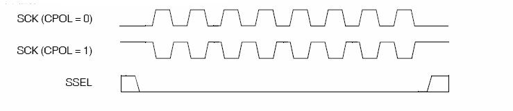
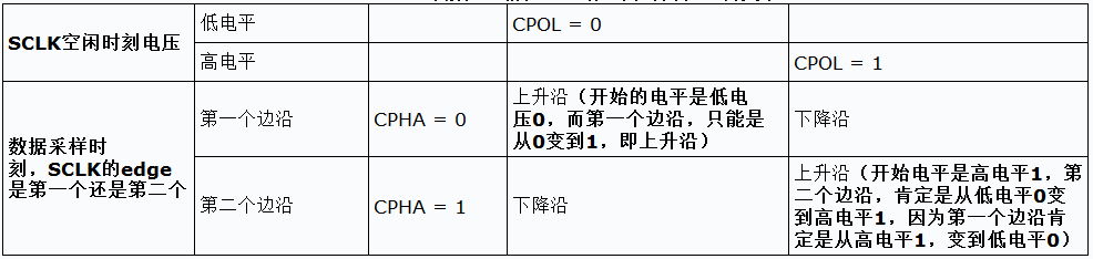
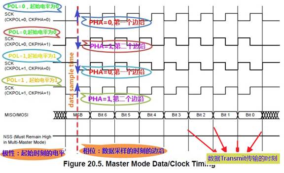
CPOL极性
先说什么是SCLK时钟的空闲时刻,其就是当SCLK在发送8个bit比特数据之前和之后的状态,
SPI的CPOL,表示当SCLK空闲idle的时候,其电平的值是低电平0还是高电平1:
CPOL=0,时钟空闲idle时候的电平是低电平,所以当SCLK有效的时候,就是高电平,就是所谓的active-high;
CPOL=1,时钟空闲idle时候的电平是高电平,所以当SCLK有效的时候,就是低电平,就是所谓的active-low;
CPHA相位
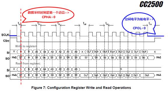
首先说明一点,capture strobe = latch = read = sample,都是表示数据采样,数据有效的时刻。
对于CPOL=0,idle时候的是低电平,第一个边沿就是从低变到高,所以是上升沿;
对于CPOL=1,idle时候的是高电平,第一个边沿就是从高变到低,所以是下降沿;
CPHA=1,表示第二个边沿:
对于CPOL=0,idle时候的是低电平,第二个边沿就是从高变到低,所以是下降沿;
对于CPOL=1,idle时候的是高电平,第一个边沿就是从低变到高,所以是上升沿;
如何判断CPOL和CPHA
(1)如何判断CPOL:SCLK的空闲时候的电压,是0还是1,决定了CPOL是0还是1;
(2)如何判断CPHA:而数据采样时刻对应着的SCLK的电平,是第一个边沿还是第二个边沿,对应着CPHA为0还是1。
此处,再多解释一下可能会遇到的CKP和CKE,其是Microchip的PIC系列芯片中的说法。
(1)CKP是Clock Polarity Select,就是极性=CPOL:
CKP,虽然名字和CPOL不一样,但是都是指时钟相位的选择,定义也一样:
CKP: Clock Polarity Select bit
1 = Idle state for clock (CK) is a high level
0 = Idle state for clock (CK) is a low level
所以不多解释。
(2)CKE是Clock Edge Select,就是相位=CPHA:
CKE: SPI Clock Edge Select bit
1 = Transmit occurs on transition from active to Idle clock state
0 = Transmit occurs on transition from Idle to active clock state
意思是
1 =(数据)传输发生在时钟从有效状态转到空闲状态的那一时刻
0 =(数据)传输发生在时钟从空闲状态转到有效状态的那一时刻
其中,数据传输的时刻,即图中标出的“数据transmit传输的时刻”,很明显,
该时刻是一个时钟和下一个时钟之间交界的地方,对应的不论是上升沿还是下降沿,
都与我们前面提到的CPHA=数据采样的时刻,的边沿方向所相反。
所以,此处的CKE,正好与CPHA相反。
所以,CKP和CKE所对应的取值的含义为:
When CKP = 0: CKE=1 => Data transmitted on rising edge of SCK, CKE=0 => Data transmitted on falling edge of SCK
When CKP = 1: CKE=1 => Data transmitted on falling edge of SCK, CKE=0 => Data transmitted on rising edge of SCK
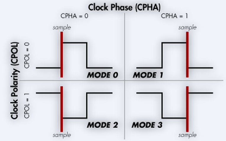
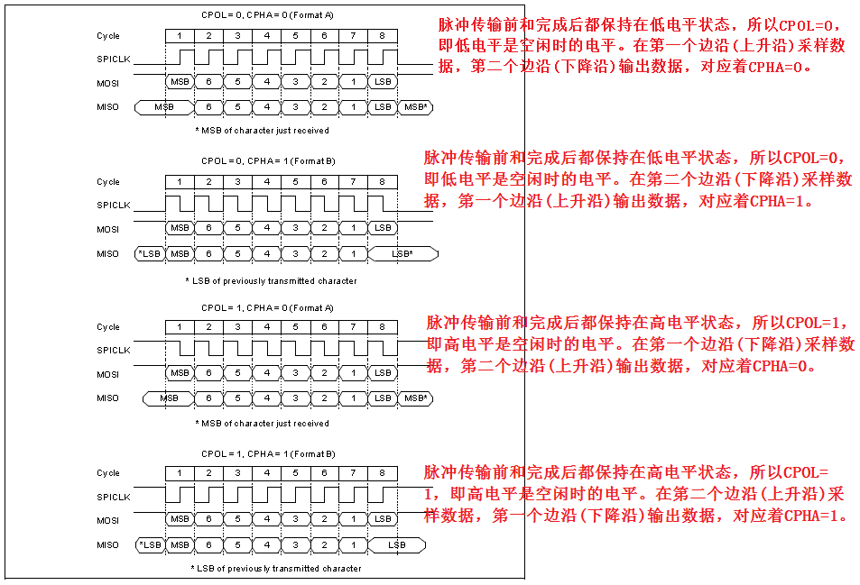
STM32F4 SPI Data clock timing diagram
Clock phase and clock polarity
Four possible timing relationships may be chosen by software, using the CPOL and CPHA bits in the SPI_CR1 register.
The CPOL (clock polarity) bit controls the steady state value of the clock when no data is being transferred.
This bit affects both master and slave modes.
If CPOL is reset, the SCK pin has a low-level idle state.
If CPOL is set, the SCK pin has a high-level idle state.
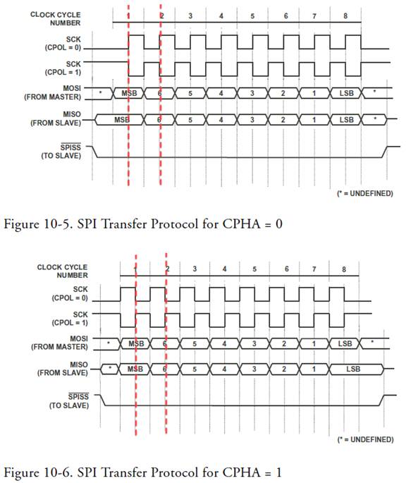
If the CPHA (clock phase) bit is set, the second edge on the SCK pin is the MSBit capture strobe.
(falling edge if the CPOL bit is reset, rising edge if the CPOL bit is set)
Data are latched on the occurrence of the second clock transition.
If the CPHA bit is reset, the first edge on the SCK pin is the MSBit capture strobe.
(falling edge if CPOL bit is set, rising edge if CPOL bit is reset)
Data are latched on the occurrence of the first clock transition.
The combination of the CPOL (clock polarity) and CPHA (clock phase) bits selects the data capture clock edge.
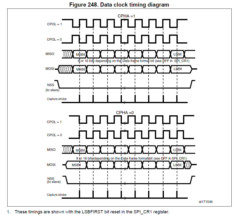
Figure 248, shows an SPI transfer with the four combinations of the CPHA and CPOL bits.
The diagram may be interpreted as a master or slave timing diagram
where the SCK pin, the MISO pin, the MOSI pin are directly connected
between the master and the slave device.
Note:
Prior to changing the CPOL/CPHA bits the SPI must be disabled by resetting the SPE bit.
Master and slave must be programmed with the same timing mode.
The idle state of SCK must correspond to the polarity selected in the SPI_CR1 register
(by pulling up SCK if CPOL=1 or pulling down SCK if CPOL=0).
The Data Frame Format (8- or 16-bit) is selected through the DFF bit in SPI_CR1 register,
and determines the data length during transmission/reception.
SPI Transfer Modes
SPI interface allows to transmit and receive data simultaneously on two lines (MOSI and MISO).
Clock polarity (CPOL) and clock phase (CPHA) are the main parameters
that define a clock format to be used by the SPI bus.
Depending on CPOL parameter, SPI clock may be inverted or non-inverted.
CPHA parameter is used to shift the sampling phase.
If CPHA=0 the data are sampled on the leading (first) clock edge.
If CPHA=1 the data are sampled on the trailing (second) clock edge,
regardless of whether that clock edge is rising or falling.
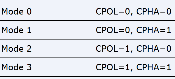
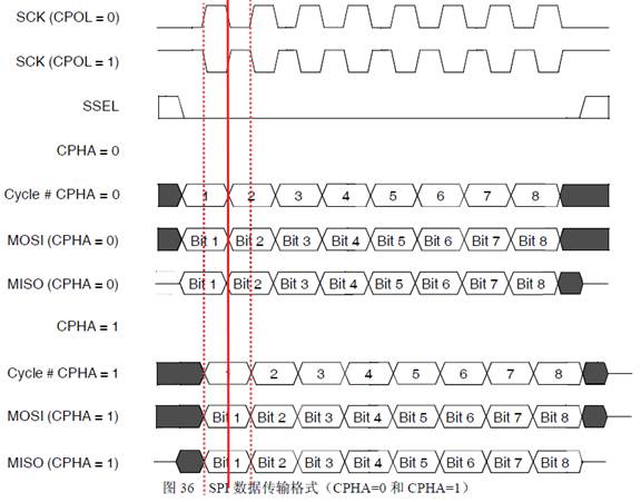
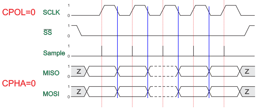
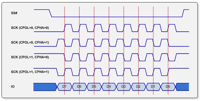
CPOL=0, CPHA=0
The data must be available before the first clock signal rising.
The clock idle state is zero.
The data on MISO and MOSI lines must be stable while the clock is high and can be changed when the clock is low.
The data is captured on the clock’s low-to-high transition and propagated on high-to-low clock transition.
CPOL=0, CPHA=1
The first clock signal rising can be used to prepare the data.
The clock idle state is zero.
The data on MISO and MOSI lines must be stable while the clock is low and can be changed when the clock is high.
The data is captured on the clock’s high-to-low transition and propagated on low-to-high clock transition.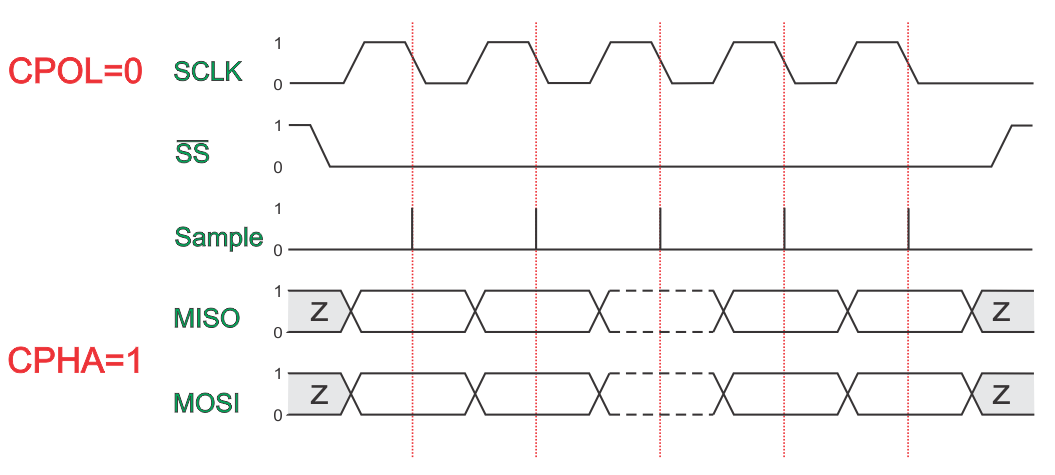
CPOL=1, CPHA=0
The data must be available before the first clock signal falling.
The clock idle state is one.
The data on MISO and MOSI lines must be stable while the clock is low and can be changed when the clock is high.
The data is captured on the clock’s high-to-low transition and propagated on low-to-high clock transition.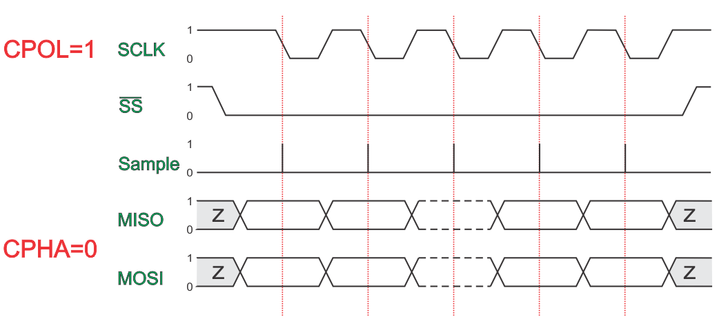
CPOL=1, CPHA=1
The first clock signal falling can be used to prepare the data.
The clock idle state is one.
The data on MISO and MOSI lines must be stable while the clock is high and can be changed when the clock is low.
The data is captured on the clock’s low-to-high transition and propagated on high-to-low clock transition.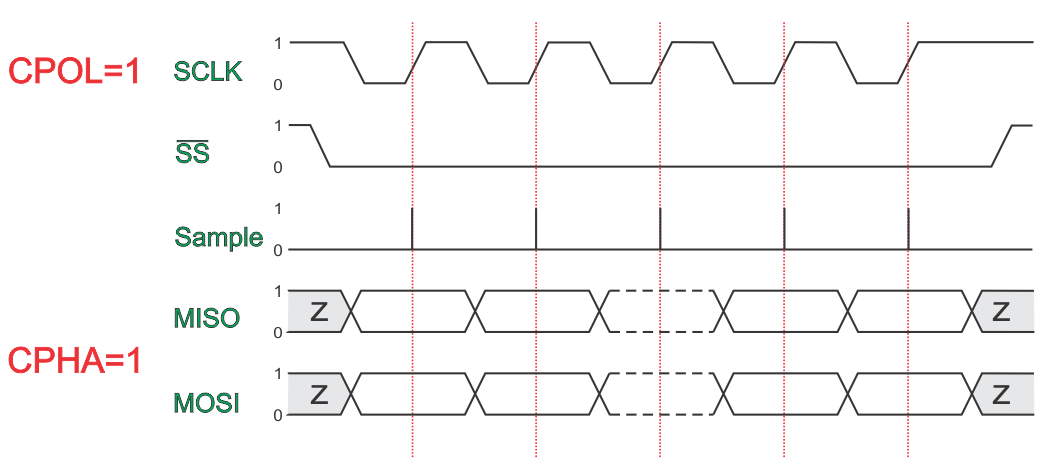
SPI Modes and Timing.
Introduction
In a lot of cases, when using SPI, we do need to use “SPI_Init_Advanced”.
It has a number of parameters. Here the parameters regarding the SPI “mode” are described. The “mode” consists of
- The SPI clock (SCK) polarity (parameter clock_idle)
- The PIC SPI data out transmit edge (parameter edge)
in
procedure SPIx_Init_Advanced(..., data_sample, clock_idle, edge: word);
The “data_sample” parameter does not belong to the actual “SPI mode”, it is an extra feature of the MCU, see here.
The SPI “Modes”
SPI knows 4 “standard” modes, reflecting the SCK’s polarity (CPOL) and the SCK’s phase (CPHA).
The definition is:
| SPI Mode | CPOL | CPHA |
|---|---|---|
| 0 (or 0,0) | 0 | 0 |
| 1 (or 0,1) | 0 | 1 |
| 2 (or 1,0) | 1 | 0 |
| 3 (or 1,1) | 1 | 1 |
The meaning is:
CPOL:
- 0 = Clock Idle low level
- 1 = Clock Idle high level
CPHA:
- 0 = SDO transmit edge (*) active to idle
- 1 = SDO transmit edge idle to active
(*): the transmit edge is the clock edge at which the SDO level changes
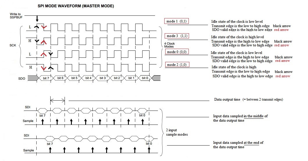
In a timing diagram this looks like(only one clock pulse shown here):
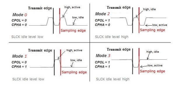
The Transmit edge is the clock edge at which the SPI output data changes,
the Sampling edge is the clock edge at which the sampling of the SPI input data takes place.
The sampling edge is normally the opposite one of the transmit edge, but see also here.
SPI and PIC/ dsPIC
The PIC MCU supports a 4 SPI modes, but the MCU registers involved are named differently and behave differently.
The 2 MCU registers are CKP (Clock Polarity) and CKE (Clock edge).
The relation between those 2 registers and the SPI modes is:
| SPI Mode | CKP | CKE |
|---|---|---|
| 0 (or 0,0) | 0 | 1 |
| 1 (or 0,1) | 0 | 0 |
| 2 (or 1,0) | 1 | 1 |
| 3 (or 1,1) | 1 | 0 |
As you can see, CKP behaves the same as CPOL, CKE is the inverse of CPHA.
This means that a simple “SPI_Set_mode” looks like this:
procedure Set_SPI_mode(CPOL_, CPHA_: byte);
// The 2 paremeters are:
// CPOL: SPI clock polarity: 0 = Clock Idle LOW;               1 = Clock Idle HIGH
// CPHA: SPI clock Phase:    0 = Transmit edge active to idle; 1 = Transmit edge Idle to active
begin
  CKP_bit := CPOL_;
  CKE_bit := (CPHA_ xor 1) and 1; // invert bit zero
end;
Above routine can e.g. used after a usage of an mE SPIx_Init… routine to (re)set the SPI mode.
The mE SPI library usage
In the mE SPI library the “SPI mode” is set by 2 parameters of the “SPIx_Init_Advanced” function.
The the parameters for PIC are : “clock_idle” and “transmit_edge”
The the parameters for dsPIC are: “clock_idle” and “edge”
Important: in both cases the last parameter (“transmit edge” or “edge” parameter) is
NOT the transmit edge, but the other one, called the “Sampling edge“,
see here. As you can see the name of the PIC parameter is wrong (it says “transmit_edge”).
Furthermore the constant values used to give the parameters their values are:
For PIC:
CPK: _SPI_CLK_IDLE_LOW and _SPI_CLK_IDLE_HIGH
CPE: _SPI_LOW_2_HIGH, _SPI_HIGH_2_LOW (**)
For dsPIC:
CPK: _SPI_CLK_IDLE_LOW and _SPI_CLK_IDLE_HIGH
CPE: _SPI_ACTIVE_2_IDLE, _SPI_IDLE_2_ACTIVE (**)
(**) Again: the “edge” is the “Sampling Edge”, not the “Transmit Edge”, see here.
Deriving the parameters from the device’s “SPI mode”
The easiest way is using the “SPI mode” if known, the hardest is deriving the parameters from the device’s timing diagram.
The table below gives the relationship between an SPI device’s “SPI mode” and the parameter values to use with “SPIx_Init_Advanced”:
| SPI MODE | clock idle parameter | Edge parameter = the “Sampling” edge |
|---|---|---|
| 0,0 | _SPI_CLK_IDLE_LOW | _SPI_LOW_2_HIGH (pic) : _SPI_IDLE_2_ACTIVE (dsPIC) |
| 0,1 | _SPI_CLK_IDLE_LOW | _SPI_HIGH_2_LOW (pic) : _SPI_ACTIVE_TO_IDLE (dsPIC) |
| 1,0 | _SPI_CLK_IDLE_HIGH | _SPI_HIGH_2_LOW (pic) : _SPI_IDLE_TO_ACTIVE (dsPIC) |
| 1,1 | _SPI_CLK_IDLE_HIGH | _SPI_LOW_2_HIGH (pic) : _SPI_ACTIVE_TO_IDLE (dsPIC) |
Important:
In mikroPascal the parameter “edge” represents the clock edge where in input data is sampled,
not the “transmit edge” (the clock edge at which the SDO data is changed).
The parameter “data sample” is not included in the “SPI mode”,
but usually “_SPI_DATA_SAMPLE_MIDDLE” will do fine, see however also here.
Defining parameters from the device’s timing diagram
This manner has to be applied if the “SPI mode” of the device at hand is not (explicitely) defined.
To find out the necessary values of the parameters we have to look to the device’s SPI timing diagram we want to handle:
Keep in mind that in the “device” diagram the “device” timing is shown.
For the PIC timing input and output should be interchanged (which was already done in the above diagram,
it shows the timing from the PIC’s perspective).
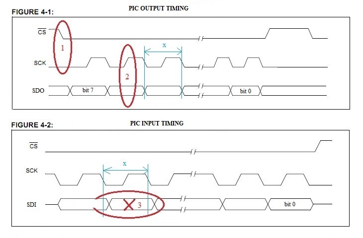
1. The “clock_idle” parameter
See 1 in the diagram. The level wanted is the SCK level at the moment notCS changes. In the diagram this level is zero, so: theclock idle is low.
This means also that (again in our case) the clock active level is high.
2. The “edge” parameter
See 2 in the diagram. The edge wanted is the one in the middle between 2 PIC output (PIC SO) datachanges (two “transmit” edges, represented by “x” in the timing diagram).
In our case we see that it is the edge from low to high, or from idle to active.
The “data_sample” parameter
The data_sample parameter is not defined in the SPI mode, it is an extra feature of the MCU.
Normally the “Sampling edge” (see here) is the opposite one of the “transmit edge”.
This is achieved by setting the “data_sample” parameter to the value “_SPI_DATA_SAMPLE_MIDDLE”.
The sampling moment can however be shifted to the same moment as the transmit edge
by setting the “data_sample” parameter to the value “_SPI_DATA_SAMPLE_END” value, see here).
How to define which one to use:
See 3 in the above diagram.
First define the “data output time”, represented by an x in the timing diagram.
It is the time from one PIC output data (PIC SO) change to the next.
Now compare the device data out (SO = PIC SI) with the “data output time”.
The data_sample value we have is the best moment in the “data output time”
the PIC should take a sample of its input data (the device output data).
In our case, the middle of the “data output time” seems to be the most appropriate (at the end would be not bad either).
Info
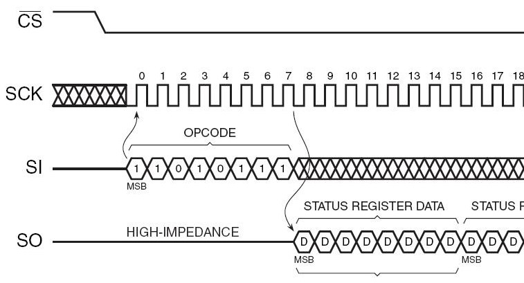
a. Timing diagram (derived and modified from Mchp datasheet)
This is the (master) timing diagram with the terms explained:
发布者:全栈程序员-站长,转载请注明出处:https://javaforall.net/109363.html原文链接:https://javaforall.net