
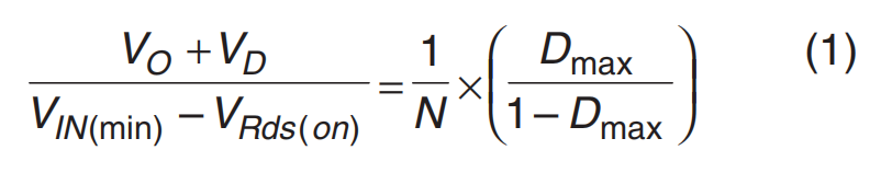

Recalculating equation (1) results in an actual Dmax of 48%.(非常重要!!!)
重新计算等式 (1) 导致实际 Dmax 为 48%。
1.Switching Frequency 开关频率
2.Transformer Design [2] 变压器设计
3.MOSFET Selection MOSFET选型
At turn on the drain current begins to flow through the FET device when the gate voltage has reached the Vgs threshold. This drain current will continue to rise until reaching its final value.Meanwhile, the drain to source voltage will remain at Vds, calculated earlier in (10).
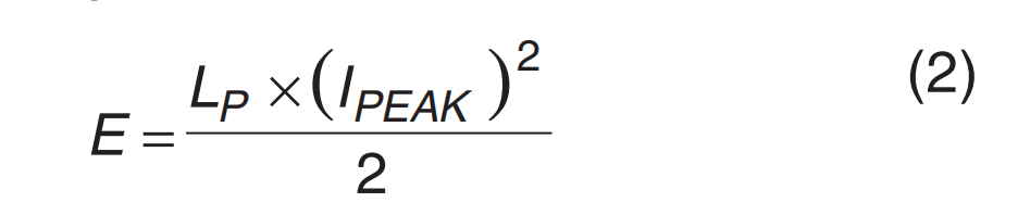
The whole process repeats itself in reverse at turn off. The power dissipation of the FET’s output capacitance, Coss, also contributes to the switching losses in the form of ½C*V^2 f.
整个过程在关闭时反向重复。 FET 输出电容 Coss 的功耗也会以 ½CV^2 *f 的形式影响开关损耗。
4.Diode Selection 二极管选型
5.input and Output Capacitors 输入输出电容器
6.SNUBBERS AND CLAMPS [7]缓冲器和夹钳 [7]
7.LC FILTER LC滤波器
版权声明:本文内容由互联网用户自发贡献,该文观点仅代表作者本人。本站仅提供信息存储空间服务,不拥有所有权,不承担相关法律责任。如发现本站有涉嫌侵权/违法违规的内容, 请联系我们举报,一经查实,本站将立刻删除。
发布者:全栈程序员-站长,转载请注明出处:https://javaforall.net/233477.html原文链接:https://javaforall.net